Tiny, Wireless, Injectable Chips Use Ultrasound to Monitor Body Processes
Columbia Engineers develop the smallest single-chip system that is a complete functioning electronic circuit; implantable chips visible only in a microscope point the way to developing chips that can be injected into the body with a hypodermic needle to monitor medical conditions
MEDIA CONTACT
Holly Evarts, Director of Strategic Communications and Media Relations
212-854-3206 (o), 347-453-7408 (c), [email protected]
ABOUT THE STUDY
The study is titled “Application of a sub-0.1-mm3 implantable mote for in vivo real-time wireless temperature sensing.”
Journal: Science Advances
Authors are: Chen Shi 1, Victoria Andino-Pavlovsky 1, Stephen A. Lee 2, Tiago Costa 1,3, Jeffrey Elloian 1, Elisa E. Konofagou 2,4, Kenneth L. Shepard 1,2
- Department of Electrical Engineering, Columbia University
- Department of Biomedical Engineering, Columbia University
- Department of Microelectronics, Delft University of Technology, The Netherlands
- Department of Radiology, Columbia University
The study was supported in part by a grant from the W. M. Keck Foundation and by the Defense Advanced Research Projects Agency (DARPA) under Contract HR0011-15-2-0054 and Cooperative Agreement D20AC00004.
Chen Shi and Kenneth L. Shepard are listed as inventors on a provisional patent filed by Columbia University (Patent Application No. 15/911,973). The other authors declare no competing interests.

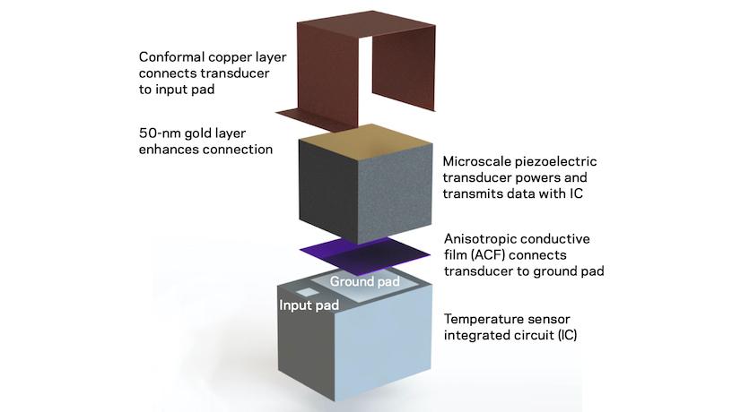
Schematic representation of the device.
New York, NY—May 12, 2021—Widely used to monitor and map biological signals, to support and enhance physiological functions, and to treat diseases, implantable medical devices are transforming healthcare and improving the quality of life for millions of people. Researchers are increasingly interested in designing wireless, miniaturized implantable medical devices for in vivo and in situ physiological monitoring. These devices could be used to monitor physiological conditions, such as temperature, blood pressure, glucose, and respiration for both diagnostic and therapeutic procedures.
To date, conventional implanted electronics have been highly volume-inefficient—they generally require multiple chips, packaging, wires, and external transducers, and batteries are often needed for energy storage. A constant trend in electronics has been tighter integration of electronic components, often moving more and more functions onto the integrated circuit itself.
Researchers at Columbia Engineering report that they have built what they say is the world's smallest single-chip system, consuming a total volume of less than 0.1 mm3. The system is as small as a dust mite and visible only under a microscope. In order to achieve this, the team used ultrasound to both power and communicate with the device wirelessly. The study was published online May 7 in Science Advances.
“We wanted to see how far we could push the limits on how small a functioning chip we could make,” said the study’s leader Ken Shepard, Lau Family professor of electrical engineering and professor of biomedical engineering. “This is a new idea of ‘chip as system’—this is a chip that alone, with nothing else, is a complete functioning electronic system. This should be revolutionary for developing wireless, miniaturized implantable medical devices that can sense different things, be used in clinical applications, and eventually approved for human use.”
The team also included Elisa Konofagou, Robert and Margaret Hariri Professor of Biomedical engineering and professor of radiology, as well as Stephen A. Lee, PhD student in the Konofagou lab who assisted in the animal studies.
The design was done by doctoral student Chen Shi, who is the first author of the study. Shi’s design is unique in its volumetric efficiency, the amount of function that is contained in a given amount of volume. Traditional RF communications links are not possible for a device this small because the wavelength of the electromagnetic wave is too large relative to the size of the device. Because the wavelengths for ultrasound are much smaller at a given frequency because the speed of sound is so much less than the speed of light, the team used ultrasound to both power and communicate with the device wirelessly. They fabricated the "antenna" for communicating and powering with ultrasound directly on top of the chip.
The chip, which is the entire implantable/injectable mote with no additional packaging, was fabricated at the Taiwan Semiconductor Manufacturing Company with additional process modifications performed in the Columbia Nano Initiative cleanroom and the City University of New York Advanced Science Research Center (ASRC) Nanofabrication Facility.
Shepard commented, “This is a nice example of ‘more than Moore’ technology—we introduced new materials onto standard complementary metal-oxide-semiconductor to provide new function. In this case, we added piezoelectric materials directly onto the integrated circuit to transducer acoustic energy to electrical energy.”
Konofagou added, “Ultrasound is continuing to grow in clinical importance as new tools and techniques become available. This work continues this trend.”
The team’s goal is to develop chips that can be injected into the body with a hypodermic needle and then communicate back out of the body using ultrasound, providing information about something they measure locally. The current devices measure body temperature, but there are many more possibilities the team is working on.
###
Columbia Engineering
Columbia Engineering, based in New York City, is one of the top engineering schools in the U.S. and one of the oldest in the nation. Also known as The Fu Foundation School of Engineering and Applied Science, the School expands knowledge and advances technology through the pioneering research of its more than 220 faculty, while educating undergraduate and graduate students in a collaborative environment to become leaders informed by a firm foundation in engineering. The School’s faculty are at the center of the University’s cross-disciplinary research, contributing to the Data Science Institute, Earth Institute, Zuckerman Mind Brain Behavior Institute, Precision Medicine Initiative, and the Columbia Nano Initiative. Guided by its strategic vision, “Columbia Engineering for Humanity,” the School aims to translate ideas into innovations that foster a sustainable, healthy, secure, connected, and creative humanity.
